


 |
310*320mm Panel Size Panel Level QFN Low Electrical Resistance
Product Details:
Get Best Price Contact Now|
Detail Information |
Product Description
Description:
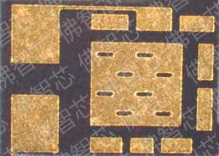
310*320mm panel size,
Chip size: 0.76*0.61mm;
Package size: 2.76*1.97mm;
Package thickness: 360um,
Application: Power management,
Process introduction:
The coming wafer is bumped with Cu post (e.g., 50 micro meters), after thining and dicing of wafer, chips with bump are picked and placed onto the temporary board. The compression molding is performed into the chips, then grinding of molded panel is introduced, PVD and LDI and semi-additive process will be continued. ABF will be used for one layer RDL manufacturing. After that, TMV will be built up for top and bottom layer connection. Finally, the surface treatment will be produced for final process. There are some variety and changes on the process if the customers want to customize their products based on the product requirements.
Applications:
Power management
Competitive Advantage:
1,Low electrical resistance , such as 0.1,0.2 mohm
2,Low power consumption
3,High efficient heat disspation
4,Thin package
5,Low price